 Nov. 15, 2012
Speckle Knife Edge Detector (SKED)
Background
SKED is an innovative technology for detecting laser ultrasonic waves on the surface of a ?rough? sample. The problem with conventional ultrasonic (non-laser) is that it requires contacting transducers to generate and detect the ultrasonic waves. This means the methods are unsuitable for inaccessible or hazardous environments. Laser ultrasonic overcomes these problems by using a laser to generate and detect the sound waves. A major problem with laser ultrasonic is detecting the waves from a rough surface.When the sample to be examined is ?rough? as many engineering components are (sufficiently unpolished that it is not a good mirror) the light is scattered randomly and conventional optical techniques will not detect the presence of sound waves passing under the optical beam. The conventional solution involves the use of highly sophisticated optical systems which are both costly and bulky often costs in the region of £80k and is a large piece of equipment. The SKED technology will cost a fraction of the above and can be retrofitted to existing equipment
Markets Sectors
This technology is a primary enabler for the use of laser ultrasonic in the Non Destructive Evaluation (NDE) market. Therefore the key market for SKED is expected to be in Non destructive testing and measurement. It is expected that the technology will form part of a laser ultrasonic measurement/detection system, such as seamless tube and composite inspection systems.The idea of using a reconfigurable chip can be further developed to be used on other non-contact techniques such as the measurement of in-plane displacements or high frequency shearography.
Technical Information
The SKED concept utilises a modified conventional knife edge detector implemented on a VLSI architecture. It quantifies the speckled reflection by measuring the changes in light intensity across knife edge to detect signals proportional to the horizontal movement of the speckles. This enables us to reorganise the light reflected from a rough surface to behave as if the reflection were from a smooth surface. The VLSI based chip configures its own architecture in response to the conditions of the reflected light.
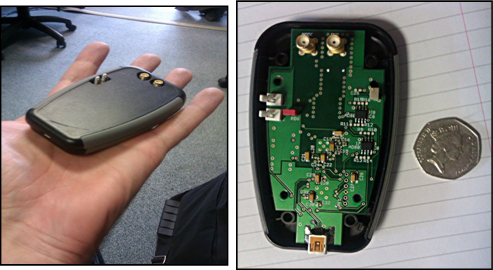
A prototype SKED design was created, and chips fabricated. The device is an array of 32x32 active photodiode pixels, used to demonstrate the detection of ultrasound on rough surface. Ability of the SKED chip to adapt to different speckle patterns was confirmed by moving the sample and examining the device configuration state.
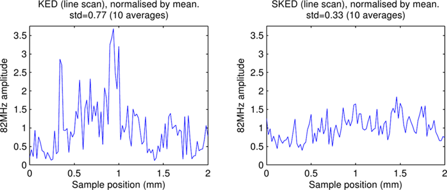
The output of the conventional KED is shown on the left, and is shown to fluctuate considerably, due to the changing speckle. In some sample locations, very little signal is present at all. On the right, the signal is much more constant, as the SKED adapts to the optical speckle at each sample location. The ideal behaviour would be a flat line at a height of 1 as shown.
The key benefit of this system is that it is able to fit in to existing microscopes while offering additional capabilities. Key benefits include:
Wide-field imaging: standard optical imaging with a lateral resolution 2-3 times better than attained with a conventional system.
Parallel confocal scanning imaging, with the equivalent of over 10,000 confocal arms operating simultaneously (currently single point and scan)
Near wide-field 3D imaging
Near wide-field STED (Stimulated emission depletion fluorescence) imaging.
由于技术保密工作限制,技术信息无法完全展现,请通过邮箱或短信联系我们,获取更多技术资料。
32x32
conventional
chip
rough
sample
sked
laser
ultrasonic
waves
speckle

![]()
![]()
![]()
 Premium